
 |
Nova DXP3600 Amplifier Test Results
Class-H Hybrid SMPS/class AB Amplifier from Nova
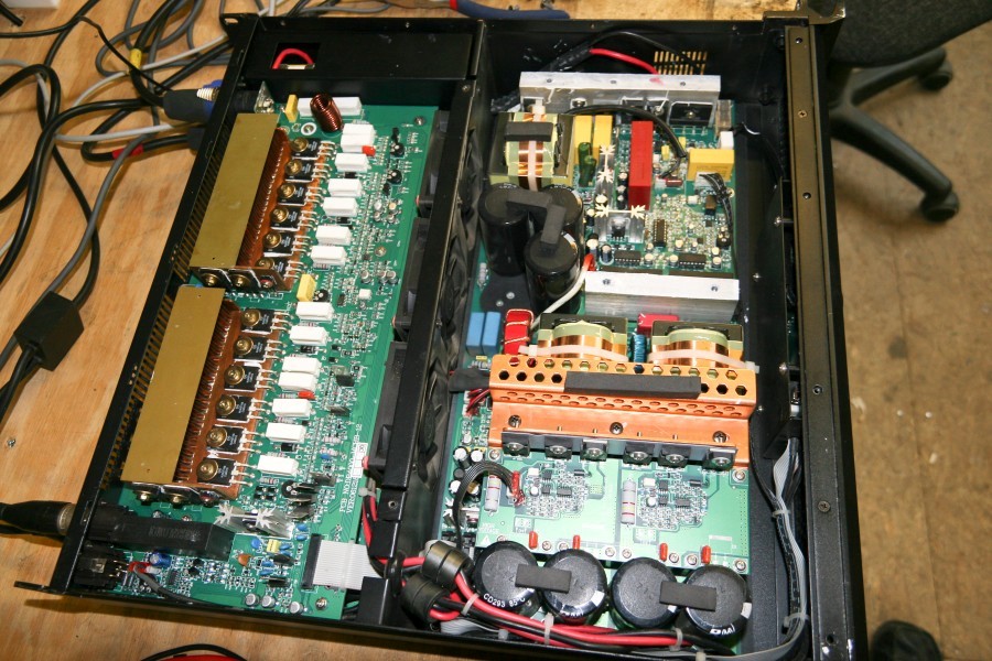
Impressively constructed amplifier from Nova features one of the largest and most complex switched mode power supplies (SMPS) we've ever seen inside an amplifier. The amp is a class-H design where the output devices operate in class-AB and the rail voltage for the output devices goes up and down with the audio signal. In this amp, this is achieved with an additional switched mode power supply bolted on to (almost literally) the secondary circuit of the primary SMPS.
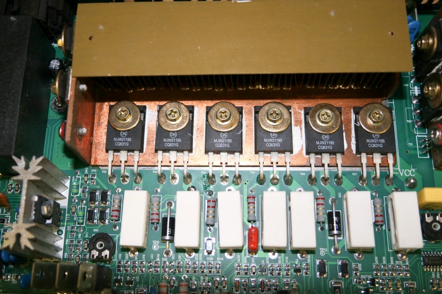
The amp has two SMPS transformers and separated rectification and smoothing capacitors for each channel, because each channel's rail voltage needs to be varied independently. This is also the reason for the very small heatsinks attached to the output devices, the idea is to minimise voltage drop across the output devices thereby reducing the amount of heat they produce, consequently reducing heatsink size and increasing efficiency. The output device heatsinks appear to be solid copper with soldered copper foil fins.
The SMPS is a power factor corrected (PFC) type, and features a huge PFC inductor. There appears to be additional secondary windings on the PFC inductor which may be used to power the circuitry of the primary SMPS, or possibly for current monitoring. The SMPS uses predominantly surface mounted components with a sprinkling of through-hole devices for the higher power stuff. The SMPS is based around a KA3525 with PFC being controlled, presumably, from a hybrid circuit within a red plastic box marked www.regal.com.cn (see photos).
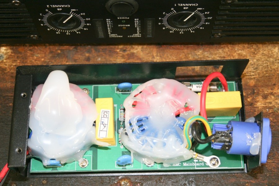
Performance of the amplifier is questionable, there is a loud whining noise at start-up from the common mode mains filtering inductors at the back of the enclosure, there is significant noise and out-of-band artefacts on the output signal, and the mains current waveform contains many high-order harmonics. The filtering inductors are made from standard hook-up wire wound round a toroidal ferrite. There has been zealous application of hot glue over the core and windings in an attempt to quell the whining noise; it is most likely caused by the windings vibrating around the core, or magnetostriction (atoms wobbling about) withing the ferrite core. This could also be the cause of the large amount of interference the amp generates and feeds back onto the mains supply - there are spurious harmonics and EMI on the current waveform - suggesting a poor quality ferrite material. (The hot glue modification may not have been done at the factory.)
It is worth noting that this amp is not brand new and has been sent to us for repair of the input filter whining noise.
The SMPS is also electrically noisy as is clear from observation of the output signal. There is significant out-of-band noise on the waveform, more than I would expect from a class-H design, but still less than some class-D designs. The amplifier delivers power into 8R load with ease, but is less astute at 4R and 2R preferring to limit to between 1/4 and 1/2 power after between 0.5 and 2 seconds. This is with continuous sine wave testing, and there is great debate as to the relevance of this when the amp is fed with a music signal. But if the amp is to be judged on its ability to handle burst or transient power, then the measurements suggest it should do fine.
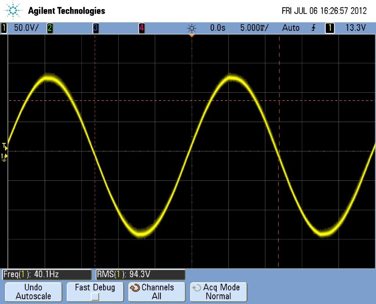
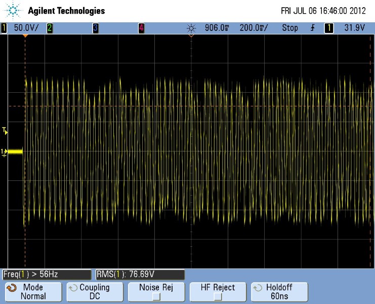
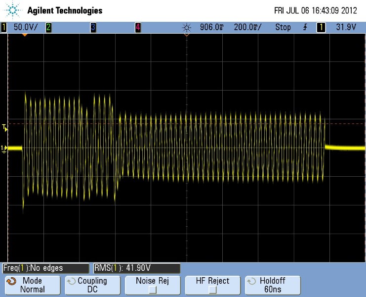
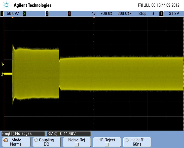
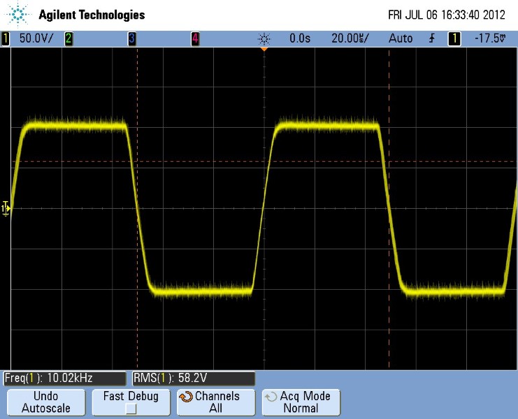
Perhaps the most troubling aspect of this amplifier is its behaviour when limiting, and indeed immediately prior to limiting. Even with a 4R load at all frequencies (less so at 10kHz), the amp goes into limiting to reduce the output current after about 1-2 seconds of full power. But during this burst period of full power, very significant distortion is present. The 40Hz 4R burst result (image 23 below) shows the signal to be periodically and completely phase reversed. It is an utter mess and not what was expected. This type of phase reversal can occur as a result of overdriving the input of an op-amp by several volts, but the input signal to the amp was well within the realms of normality when this happened. It happens on both channels too. In total honesty I cannot think of a reason for this dramatic result, it warrants further investigation.
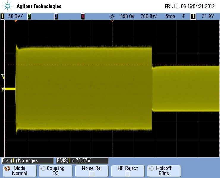
The action of the limiter is very hard. When the amp limits, the power is immediately dropped off to the reduced value (see burst images below) and then the output is brought up to full level immediately after a few seconds where the cycle repeats. The level is not gradually reduced or increased, it happens almost instantaneously.
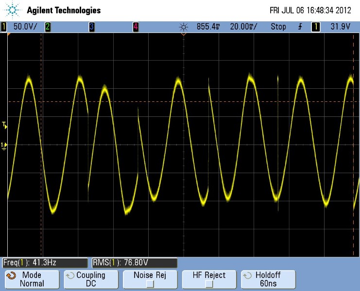
At 10kHz, 4R, the action of the amplifier before the limiter kicks in is better, I couldn't find any phase reversal within the trace. But the action when limiting is much different. The limiter hard clips the waveform turning it into something resembling a square wave. See photo 37 below. This clipping persists for as long as the amp is in limit. Again, this behaviour is very much undesirable and warrants further investigation.
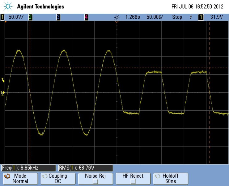
Because of the action of the limiter, two power ratings are given in the table below for 4R and 2R loads. The upper figure in the table is the burst power, available for between 0.5 seconds (2R) and 2 seconds (4R), and the lower figure is the power after limiting. No 10kHz 2R rating was attempted.
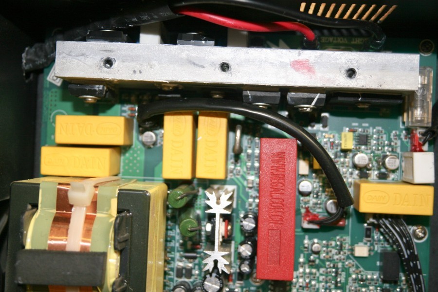
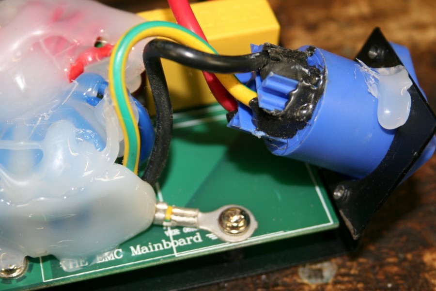
There is also a potential safety concern with regard to the way the mains earth is connected to the amplifier chassis. See image 11 below. The earth cable out of the back of the mains connector is connected to the mains filter enclosure through the back of a single small screw that holds down the input filter PCB. The ring terminal is not in direct contact with the enclosure. Also, the earth goes to the input filter enclosure and not directly to the main chassis. The filter enclosure is fixed in to the chassis with three other screws, but the mating surfaces of the chassis and enclosure are painted. In other words, the main earth is connected to the chassis through the back of a small PCB screw and some painted metal. It's connected, just not very well.
Mains voltage connected to scope with an Agilent N2790A differential probe, current measured with an Agilent N2781B current probe. Audio signal waveforms are shown on an Agilent MSO7104B 1GHz oscilloscope with mains waveforms simultaneously captured on an Agilent MSOX3054A 500MHz oscilloscope.
|
All results taken with sine wave input into a resistive dummy load of 8, 4 and 2 ohms (where applicable), two channels simultaneously driven (unless otherwise stated), at the threshold of clipping. These results should be considered maximum 'continuous RMS' power ratings (>5 seconds). Distortion measurements, labelled THD%, are taken with an HP8903A audio analyser (80kHz Bandwidth). | |||||||||||||||||||||||||||||||||||
| Manufacturer | Nova |
|---|---|
| Model | DXP3600 |
| Weight | 12.5 kg |
| Power to weight Ratio1 | 269.7 W/kg |
| Notes | Mains voltage hovered around 238V throughout the test, dropping to around 233V under 2R loading. Tested on 6th July 2012. |
| Manufacturer's Website | http://www.novacoustic.com/ |
1 Power to weight ratio is calculated by taking the average of the power measurements at 4 ohms, multiplying by the number of driven amp channels, and then dividing this value by the weight of the amplifier.
Click the images below for full-size versions


Description of Images:
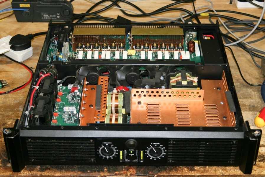
- Amplifier internals showing power supply at the front of the enclosure and amp channel 2 at the back. Channel 1 is under channel 2. The amplifier is assembled 'upside-down' in its case. The heatsinks for the output devices are copper but the power supply heatsink is gold-anodised aluminium.
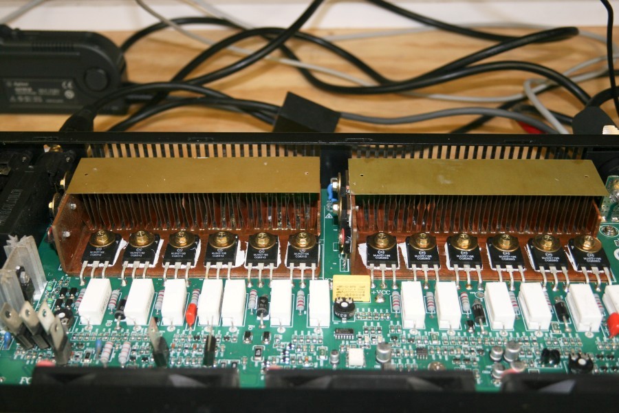
- Channel 2 at the back of the amp. Note the very small size of the output device heatsink - the amp's power supply varies with the input signal to minimise dissipation across the output devices. Mains filtering is at the extreme right, the fuse on the mains filter PCB is just visible.
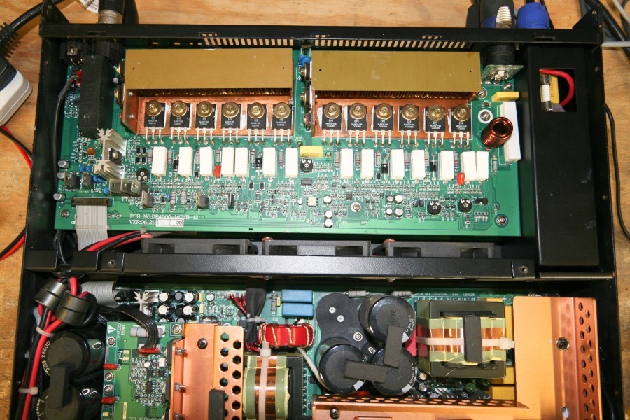
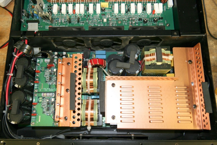
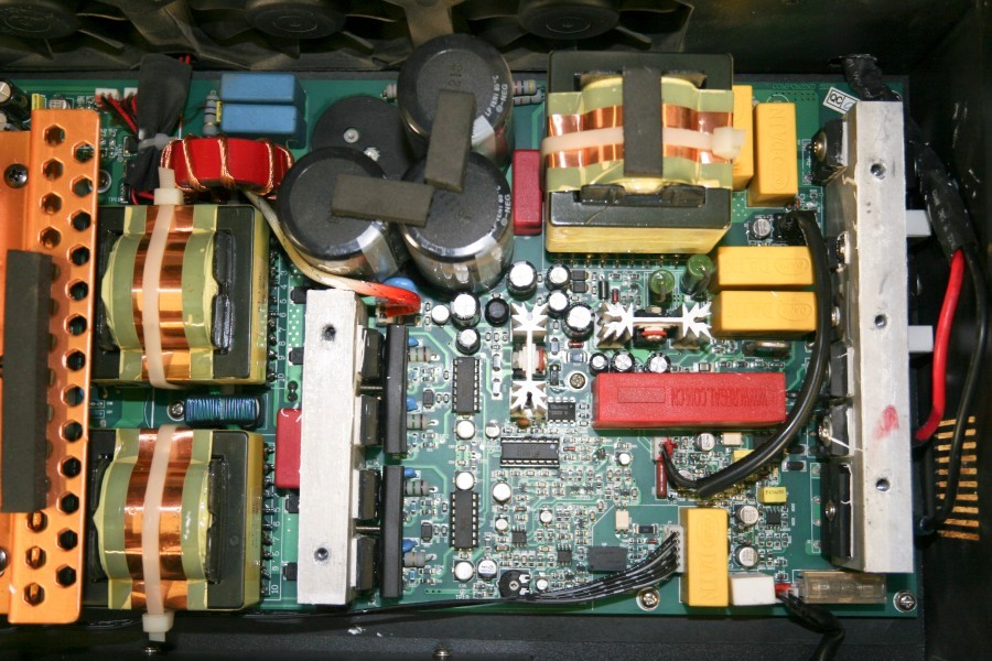
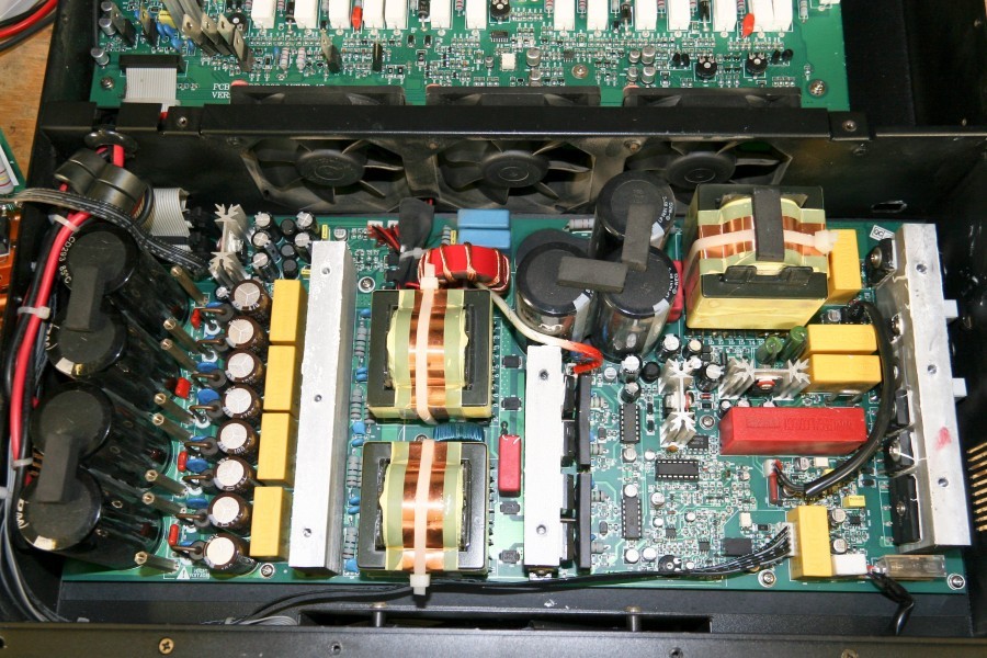
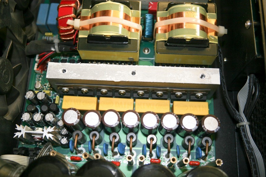
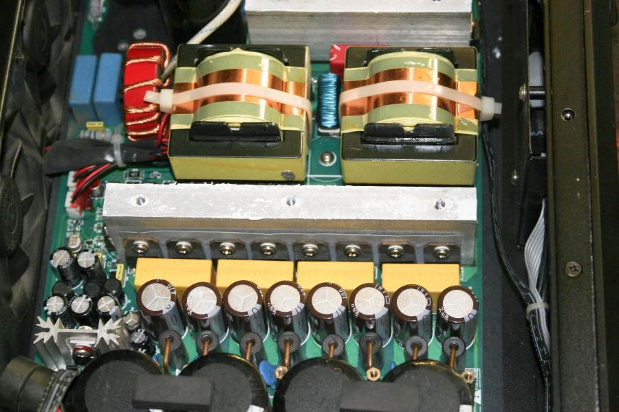
- Power supply and three cooling fans. Primary bulk storage capacitors are at the centre-right, secondary smoothing caps are at the extreme left. The power factor correction inductor is to the right of the primary caps.
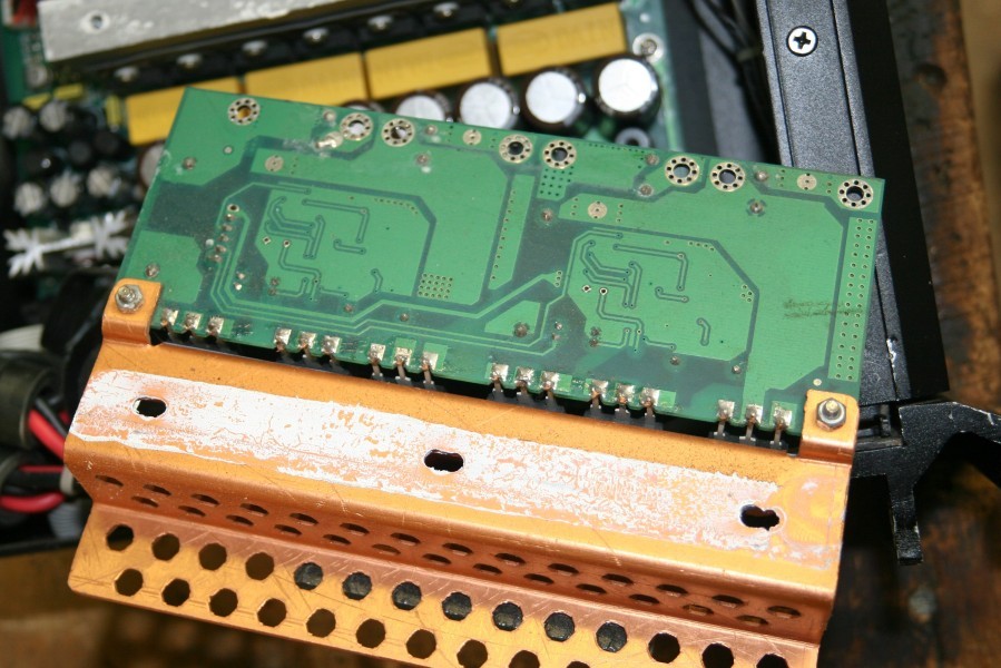
- Secondary rectifier PCB mounted above the mains PCB. This PCB is a 4-layer board.
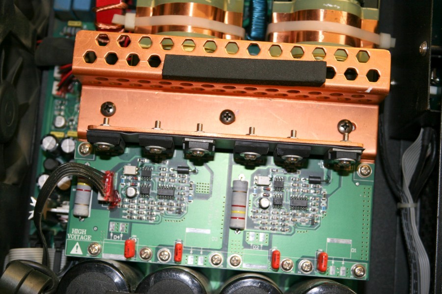
- Closeup of one half of channel 2's output devices. High quality ON semiconductor parts are used and mounted directly to the copper heatsink.
- Showing the copper heatsinks and copper fin design. The fins are soldered to the copper base and insulating material is placed on top to isolate the live heatsinks from the case.
- Power supply with the gold heatsink removed. One of the most complex switched-mode power supplies I've seen inside an amplifier. Primary rectification and PFC control devices are mounted on the aluminium block to the right. The PFC inductor is centre-top and is absolutely huge. The SMPS transformers are at the left, one per channel, and the primary switching devices are mounted on the smaller aluminium block next to them. High quality Ixys devices are used throughout, and the SMPS is based around a KA3525 with IR2110 gate drivers.
- Closeup of the PFC controller devices and primary rectification. The big red plastic box says www.regal.com.cn on it and appears to be a hybrid circuit, possibly some kind of PFC controller. (A visit to their website suggests they sell audio equipment). The PFC inductor is bottom left.
- Another shot of the amplifier. The power supply takes up more case volume than the amp channels.
- Input filter PCB. Somebody has tried to cure the whistling inductor problem by studious application of anti-whistle adhesive (hot glue). The common mode chokes are wound with normal mains cable. Note the PCB is enclosed in its own metal case which is then screwed into the enclosure (remember this for the next image).
- Main earth terminal direct from the Powercon socket is connected through the PCB. Not only that, but the earth is 'connected' only to the metal enclosure around the power supply filter, not direct to the amp chassis. This in turn is screwed to the amp chassis with three screws through painted metal. In short, the entire amplifier is earthed through a bit of PCB and some painted metal. It might be enough to pass a PAT test, but is less than satisfactory in my opinion. In addition, the crimped end of the earth terminal sits directly over the PCB track carrying the mains neutral. The thin layer of green PCB lacquer is all that stops it making contact.
- Another shot of the power supply with the heatsink and rectifier PCB removed. The PFC controller devices are not in close proximity to the PFC inductor causing possible elevated interference.
- Showing secondary side switching devices underneath the rectifier PCB. This appears to be an additional SMPS after the main SMPS to vary the rail voltage.
- Another shot of the secondary switching devices. High quality ST parts are used.
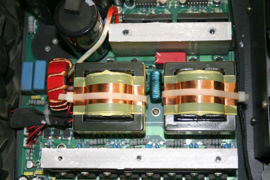
- Pair of power transformers
- Underneath the rectifier PCB - a 4-layer board. The rectifier PCB is mounted on metal stand-offs which double as connections to the main PCB. The large path length between the rectifiers and secondary SMPS could cause increased interference.
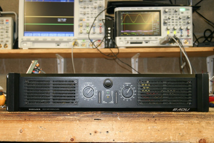
- Front of the amp (upside-down) on the bench.
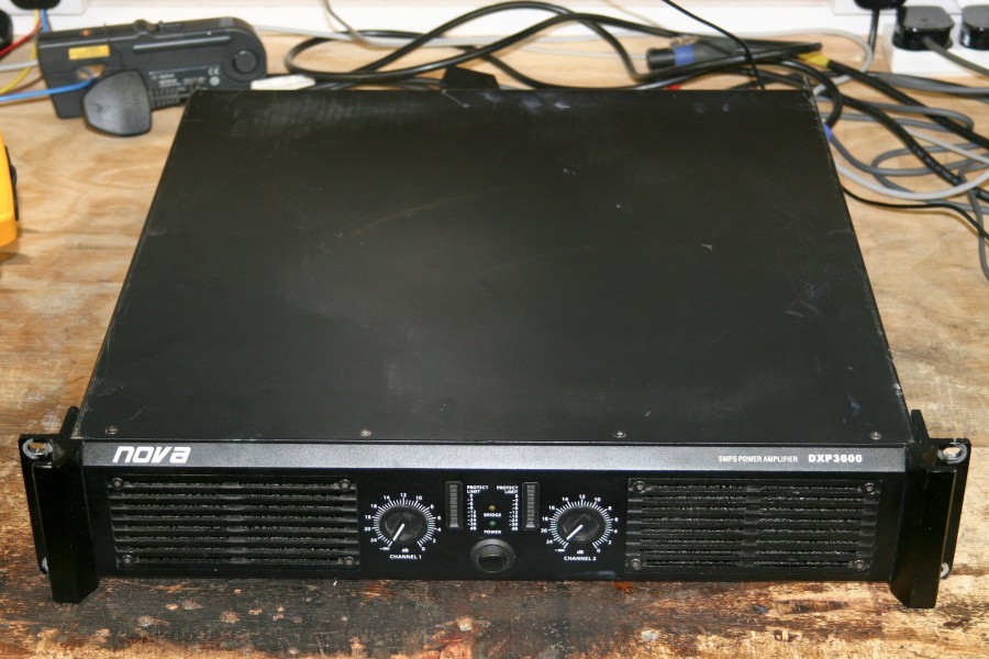
- Amplifier on the bench, right way up.
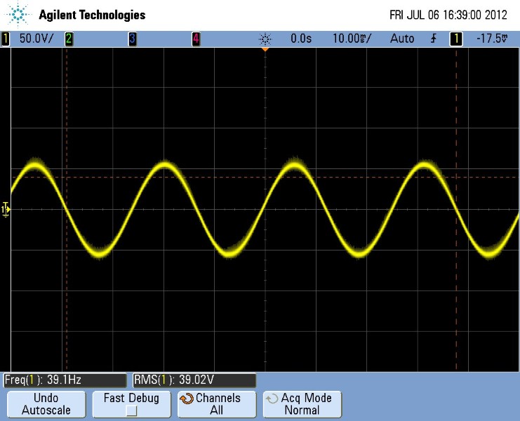
- 40Hz, 8R sine wave. Some evidence of clipping, and the waveform appears slightly furry due to out-of-band noise from the SMPS getting into the audio signal.
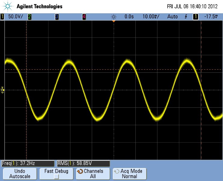
- 40Hz, 4R sine wave, before limiter cuts in. Slightly furry waveform.
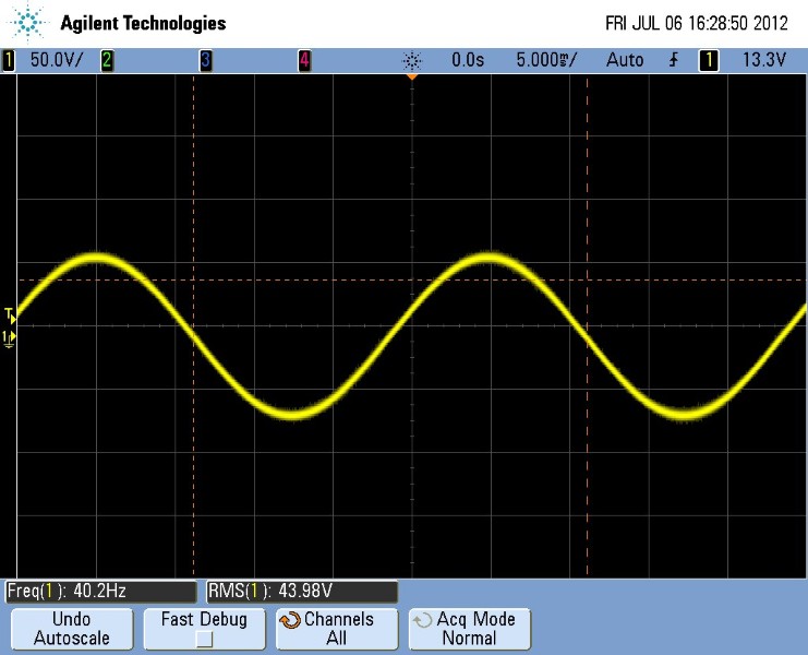
- 40Hz, 4R sine wave, after limiter cuts in (about 2 seconds)
- 40Hz, 4R sine wave, burst power. Amplifier distorts severely when not in limit (see next photo)
- 40Hz, 4R sine wave, burst power, (zoomed in version of previous image). Note the dramatic periodic phase reversal akin to overdriving a poor quality op-amp.
- 40Hz, 2R sine wave, before limiter cuts in.
- 40Hz, 2R sine wave, after limiter cuts in (about 0.5 seconds).
- 40Hz, 2R sine wave, burst power. Severe distortion artefacts when not in limit.
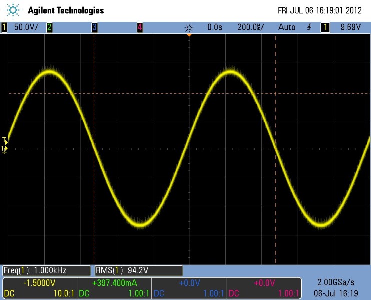
- 1kHz, 8R sine wave.
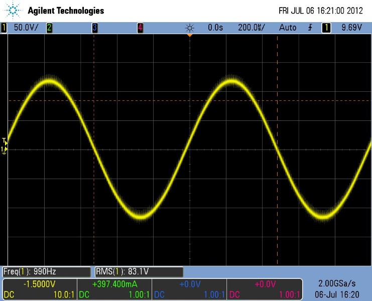
- 1kHz, 4R sine wave, before limiter cuts in. Visible out-of-band noise.
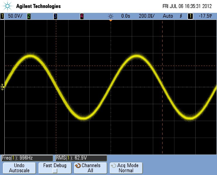
- 1kHz, 4R sine wave, after limiter cuts in (about 1.5 seconds).
- 1kHz, 4R sine wave, burst power. Distortion artefacts present when not in limit.
- 1kHz, 2R sine wave, before limiter cuts in.
- 1kHz, 2R sine wave, after limiter cuts in (about 0.5 seconds).
- 1kHz, 2R sine wave, burst power. Distortion artefacts present when not in limit.
- 10kHz, 8R sine wave, at clipping. Slight distortion on waveform crests.
- 10kHz, 8R sine wave, just prior to clipping. Waveform crests much cleaner.
- 10kHz, 4R sine wave, burst power. Little distortion this time when not in limit, but...
- ...zoomed in version of previous image showing the point at which the limiter cuts in. Severe clipping during limit.
- 10kHz 8R square wave, full power. Very good, no overshoot or undershoot and relatively fast and symmetrical rise and fall times.
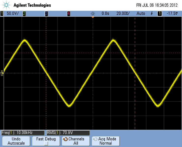
- 10kHz 8R triangle wave, full power. Very good symmetry.
- Quiescent noise and DC (no input). Channel 1 noisier than 2. Shows bursts of RF caused by bleed-through of power supply noise.
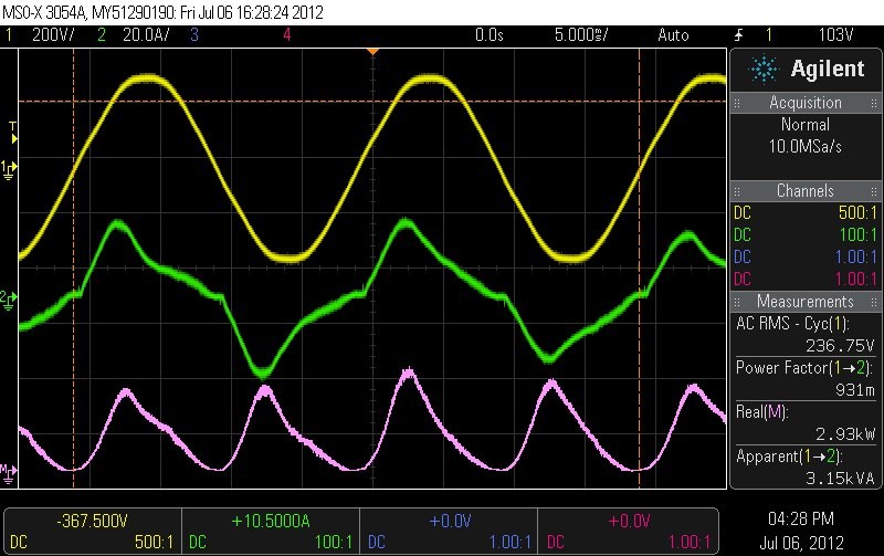
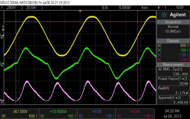
- 40Hz, 8R, mains waveforms. Yellow trace is mains voltage, green is mains current and pink is instantaneous power. Power factor is good, although there is still a fair bit of harmonic current distortion.
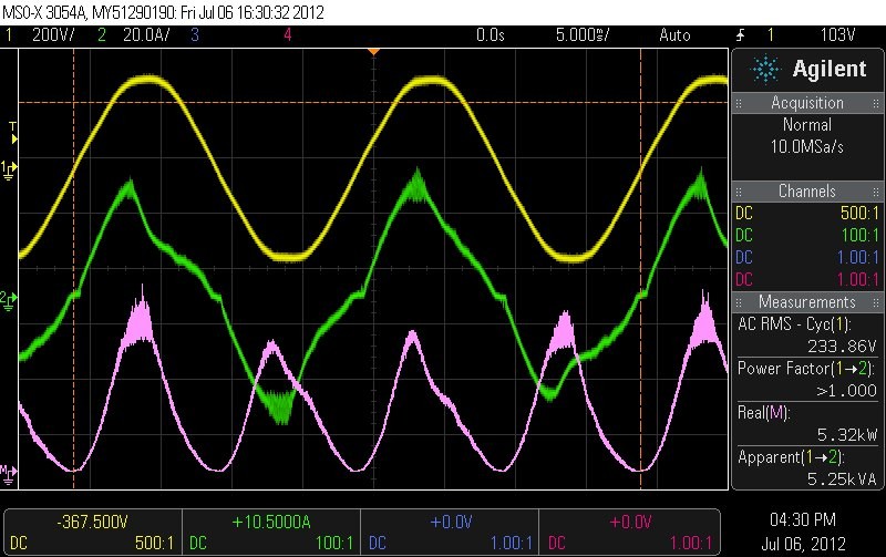
- 40Hz, 4R, pre-limit mains waveforms. Yellow trace is mains voltage, green is mains current and pink is instantaneous power. (Power factor result and instantaneous power waveform here is incorrect, the screen capture must have happened as the scope was calculating the value). Note the high frequency current harmonics on the waveform crests.
- 40Hz, 4R, post-limit mains waveforms. Clean-ish current waveform.
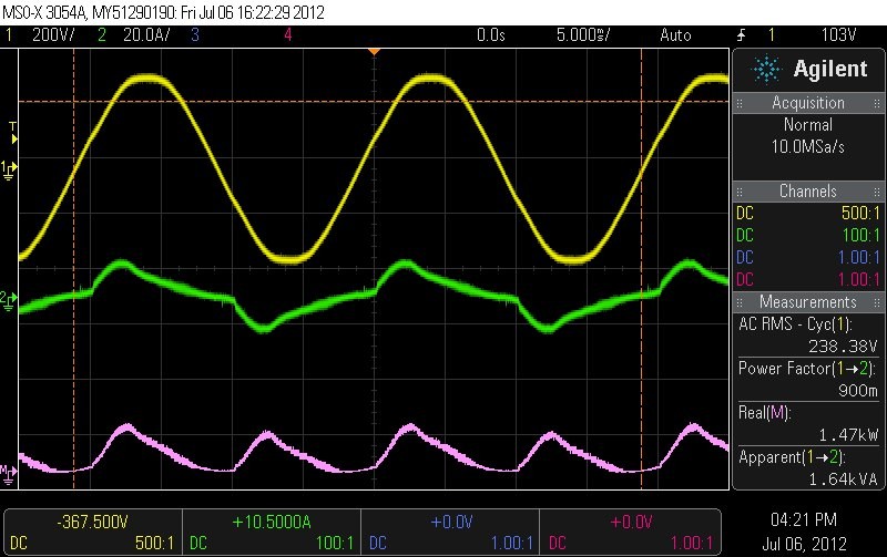
- 1kHz, 8R mains waveforms. Similar to the 40Hz case.
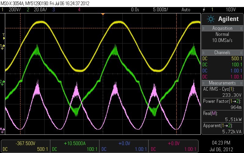
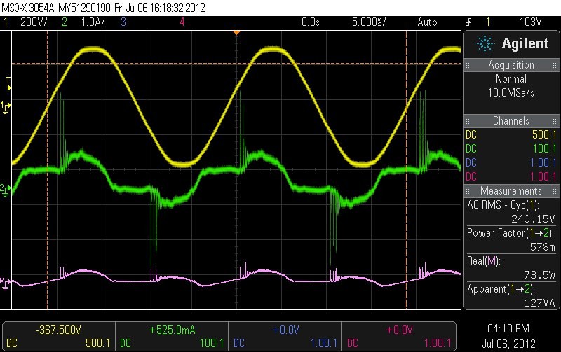
- 1kHz, 4R, pre-limit mains waveforms. Note the high frequency current harmonics on the waveform crests.
- 1kHz, 4R, post-limit mains waveforms. Clean-ish current waveform.
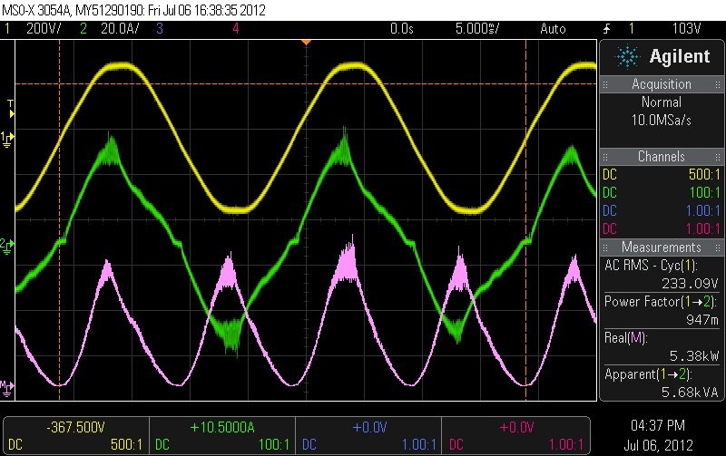
- 1kHz, 2R, pre-limit mains waveforms. Note the high frequency current harmonics on the waveform crests.
- 1kHz, 2R, post-limit mains waveforms. Note the high frequency current harmonics on the waveform crests.
- 10kHz, 8R, mains waveforms. Clean-ish current waveform.
- Low power mains waveform (1kHz, 8R, approx 10W output per channel). Vertical scale of the current waveform has been magnified compared to revious waveforms. Note the high frequency current spikes around the zero-crossing of the voltage waveform, and HF harmonics present at the waveform crests.
- Quiescent mains waveform (no input, no load). Vertical scale of the current waveform has been magnified compared to revious waveforms. Even higher current peaks around the voltage zero-crossings, but lower peaks at waveform crests compared to the previous image. Potential EMI concern here, possibly due to inadequate mains filter design.
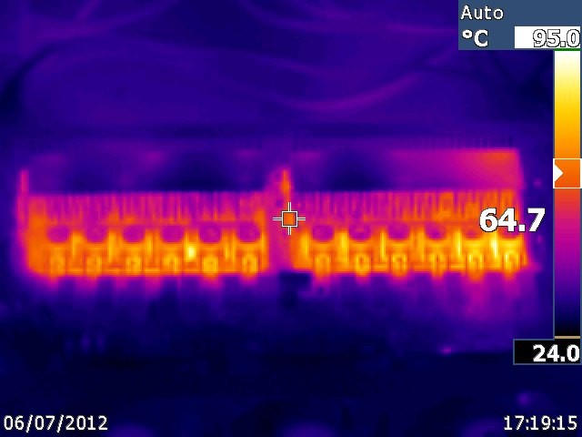
- Thermal image of the output devices and heatsinks, 8R, 1kHz, half power, 10 seconds (lid removed, no airflow). The two transistors on the far right seem to be hogging current, but otherwise good thermal distribution.
- Thermal image of the rectifier PCB. Rectifier diodes running cool, transformers at the top of the image running warm, but nothing untoward.
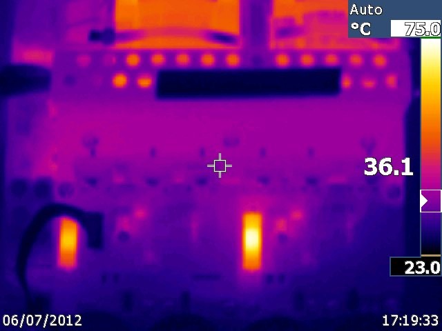
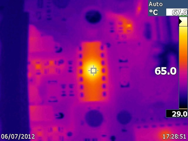
- Thermal image of main SMPS primary side. IR2110 gate drivers are visible towards the left.
- Thermal closeup of one of the gate drivers running comparatively cool.
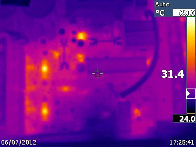
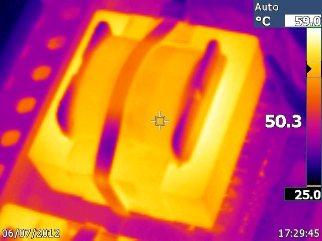
- Thermal image of one of the SMPS transformers, 8R, 1kHz, half power, 10 seconds. Running warmer than expected, may suggest some core losses.
